For most of human history, our inventions and innovations have been at a scale that’s literally easy to grasp. From the largest cathedral to the finest pocket watch, everything that went into our constructions has been something we could see with our own eyes and manipulate with our hands. But in the middle of the 20th century, we started making really, really small stuff: semiconductors. For the first time, we were able to create mechanisms too small to be seen with the naked eye, and too fine to handle with our comparatively huge hands. We needed a way to scale these devices up somewhat to make them useful parts. In short, they needed to be packaged.
We know that the first commercially important integrated circuits were packaged in the now-familiar dual in-line package (DIP), the little black plastic millipedes that would crawl across circuit boards for the next 50 years. As useful and versatile as the DIP was, and for as successful as the package became, its design was anything but obvious. Let’s take a look at the dual in-line package and how it got that way.
The history of the DIP is shrouded in mystery, which is somewhat unusual for an industry that trumpets innovations far and wide and routinely patents everything. There’s even some doubt as to who the actual inventor or inventors were. The consensus seems to fall on three employees of Fairchild Semiconductor: Don Forbes, Rex Rice, and Bryant “Buck” Rogers, and a credible source, the Computer History Museum, backs up that assertion.
The three are said to have designed the package in 1964, specifically to house new IC dies with ever-increasing numbers of pins needed to support power and signals. Early chips were housed mainly in either TO-5 or TO-18 packages that were more commonly used to package bipolar transistors. The metal cans worked fine for 3-lead devices, but scaling them up to provide more and more connections proved to be limiting. The can could only be made so large, and the radial leads could only be packed so tight. Ten leads were about the practical limit, and that would not support the more complicated chips in the pipeline.
We also know that the Fairchild team’s design is a direct descendant of the ceramic flatpack design that had been developed for the US military as a standard for surface-mount integrated circuits. The package was the brainchild of Yung Tao, a Texas Instruments who devised the ceramic package in 1962. The design of the package was tailored by the military’s need for vibration resistance, a hermetic seal against environmental intrusion, and heat dissipation. The package looks somewhat like a DIP with the leads flattened out into a plane to accommodate surface mounting rather than through-hole mounting.
We don’t have a lot of literature that reveals the design goals for the DIP, but it’s clear from Fairchild marketing material aimed at the industry that Forbes, Rice, and Rogers were tasked with making improvements to the basic concept of the flatpack package with an eye to the growing consumer market. Ease of handling for electronics manufacturers, relative both to flatpacks and to assembling circuits from discrete components, was touted as a selling feature. Providing a package that would be easily handled for board-stuffing was key, too, since Fairchild listed “dimensional tolerances to fit holes drilled to commercial standards” as another feature. These marketing points would probably have driven the lead spacing and the size requirements, as well as overall package size.
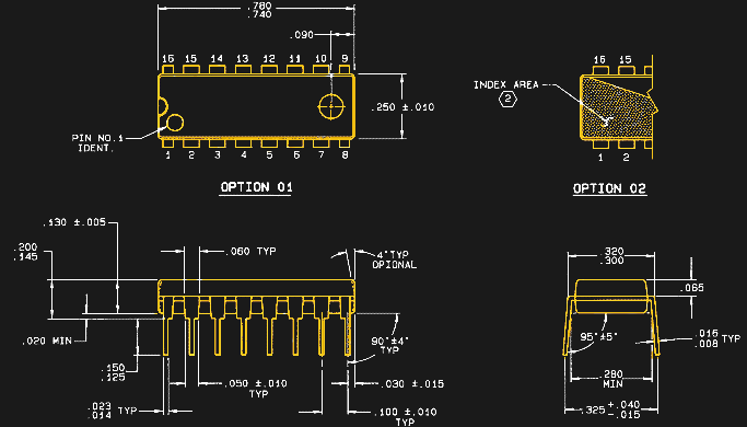
While not suggested by the advertising, ease of PCB layout was also likely a design criterion. With circuit complexity increasing, component counts on boards were bound to jump dramatically; getting power to all those chips and routing their signals around the board would soon start becoming a problem. The DIP design, with pins spaced 0.1″ (2.54 mm) apart, left plenty of room for PCB traces to be routed between pins, and the 0.3″ (7.62 mm) spacing between rows of pins offered room for traces

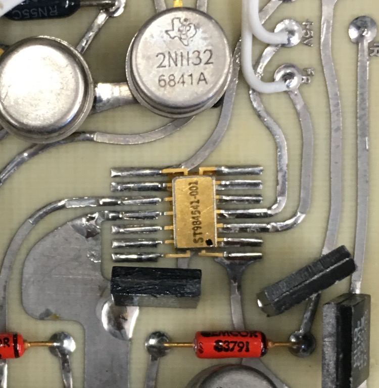
Field serviceability was also a selling point mentioned in the marketing literature. That feature no doubt came as a result of what was probably the overriding design goal: cheap, rapid manufacturing methods. Inside the DIP package, the IC die itself is mounted to a metal assembly called the lead frame. The lead frame is easily formed by a progressive stamping press, in which a series of dies punch the part out of a continuous coil of sheet metal stock. The lead frames can be stamped, the dies affixed, the die pads bonded to the leads by ultrafine wires, and the assembly encapsulated in one continuous process. Folding the leads down perpendicular to the device’s body is the final step, and leaves the leads exposed at the top of the chip, allowing access to testing instruments.
Following these design goals, devices in the dual in-line package started hitting the market in 1965. Fairchild originally concentrated on ceramic encapsulation, in an attempt to provide the same hermetic seal specified by the military for their devices. Later, encapsulation in plastic resin was introduced for less stringent environmental regimes, which drove the unit cost down drastically.
As a result of great design, low cost, and support for increasingly complex dies, the DIP was a wildly successful package for most of 50 years. Its basic design was extended to support more leads and larger dies, but eventually, technology surpassed the venerable design, and by the late 2000s some new chips were no longer available packaged in DIPs. The PCB world may be ruled by surface mount devices now, but that would not be the case if the design of Forbes, Rice, and Rogers hadn’t paved the way.
The Dual In-Line Package and How It Got That Way
Source: HackADay