When it comes to reverse engineering silicon, there’s no better person to ask than Ken Shirriff. He’s the expert at teasing the meaning out of layers of polysilicon and metal. He’s reverse engineered the ubiquitous 555 timer, he’s taken a look at the inside of old-school audio chips, and he’s found butterflies in his op-amp. Where there’s a crazy jumble of microscopic wires and layers of silicon, Ken’s there, ready to do the teardown.
For this year’s talk at the Hackaday Superconference, Ken walked everyone through the techniques for reverse engineering silicon. Surprisingly, this isn’t as hard as it sounds. Yes, you’ll still need to drop acid to get to the guts of an IC (of course, you could always find a 555 stuck in a metal can, but then you can’t say ‘dropping acid’), but even the most complex devices on the planet are still made of a few basic components. You’ve got n-doped silicon, p-doped silicon, and some metal. That’s it, and if you know what you’re looking for — like Ken does — you have all the tools you need to figure out how these integrated circuits are made.

The first question you might ask when decapping a chip is how to get the silicon out of the chip. For some 555 timers, this is easy. You can indeed still buy 555s in a TO-99 metal case, and with a jeweler’s saw, hack saw, or even a dremel, that metal can will come right off, revealing the juicy silicon nougat inside.
For other chips, you’ll need to do a bit more work. After removing the bulk of the material, Ken uses a product called Armor Etch to remove some silicon dioxide. Armor Etch apparently comes from craft stores, used to etch glassware with silhouettes of birds or the words ‘live laugh love’. To remove metal layers, it’s just a matter of a few drops of hydrochloric acid. Of course, Ken’s talk was only a survey of decapsulation, the best info comes from John McMaster’s wiki. With the chip decapsulated, it’s mounted in a metallurgical microscope equipped with an XY stage and a webcam that Ken picked up on eBay for a few hundred dollars.
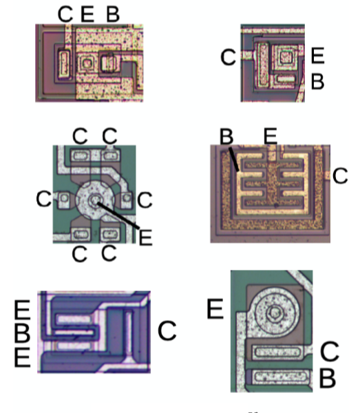
But once you get that chip under the scope, how do you reverse engineer the circuit. There are only a handful of parts — transistors, resistors, and capacitors — that go into the layers of silicon, but even a transistor can look vastly different from one process or manufacturer to another. Luckily, Ken has been doing this a while, and he’s got an eye for what these things look like.
Transistors can look like circles, squares, or other interesting geometric patterns. Resistors, though, are usually just long lines of silicon underneath the metal layer. Tie all this together, and you can start to see pattern emerging. If you find two transistors with the base wired to the collector of each other, you’ve probably got a flip-flop. If you see rows and columns of transistors, you probably have some sort of data ready to be decoded.
It’s no exaggeration to say that Ken Shirriff is one of the best at what he does. He’s neck deep in making the innards of semiconductor devices understandable to everyone, and it shows: every single time Ken posts his latest discovery on his blog, it’s quickly upvoted to the top of Hacker News and makes the rounds on the cool parts of Twitter. This talk is a great look at the techniques Ken uses to understand these die shots, and a must-watch for everyone who even has an inkling of interest in modern semiconductor devices.
Ken Shirriff Explains His Techniques For Reverse Engineering Silicon
Source: HackADay