Many readers are certainly familiar with the process for home-etching of PCBs: it’s considered very straightforward, if a little involved, today. This was not the case in my youth, when I first acquired an interest in electronics. At that time, etching even single-sided boards was for “advanced” hobbyists. By the time I started etching my own PCBs, the advanced hobbyists were on to double-sided home-etched boards — the only type not pictured above, because I couldn’t find the one successful example I ever created. I later saw the rise of “bare bones” fabricated PCBs: professionally made fixed size boards with plated-through holes, but no soldermask or silkscreen. Eventually, this gave way to the aggregating PCB services we have now with full two-layer boards, complete with soldermask and silkscreen.
Today, the “advanced” hobbyist may be using four-layer boards, although the four-layer adoption rate is still relatively low – OSH Park produces around 90% two-layer and 10% four-layer, for instance. I think this will inevitably increase, as has been the case with all the previous technologies: the advanced eventually becomes the mainstream. Each of the previous shifts has brought easier design and construction as well as improved performance, and the same will be true as four layers becomes more commonplace.
So, let’s take a look at designing four-layer PCBs. If you’ve never considered one for any of your designs, you may be pleasantly surprised at what little extra cost is involved for all the benefits you gain.
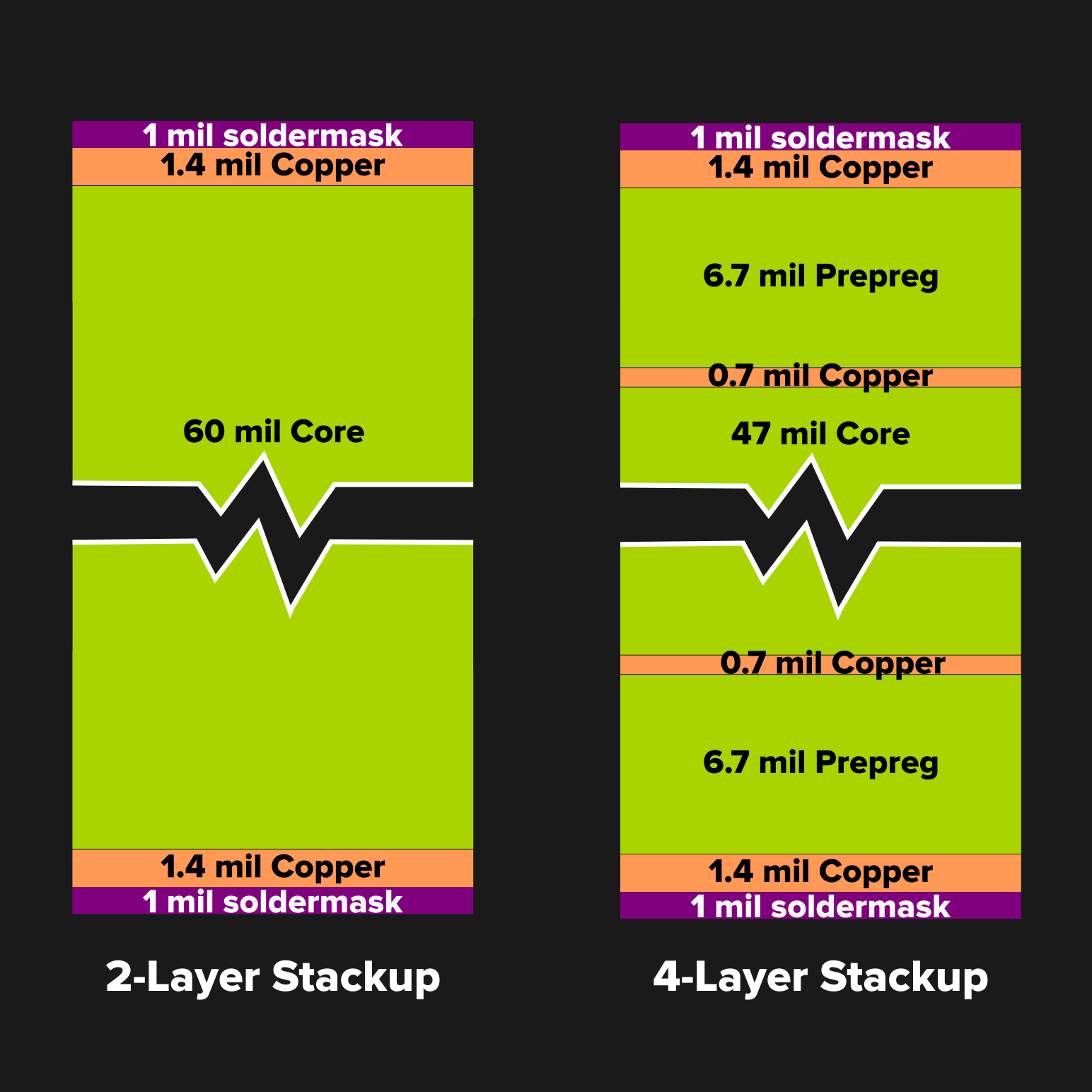
The obvious difference between two-layer and four-layer PCBs is two extra layers of copper. The particular arrangement of the layers within a board is known as a “stackup.” Two-layer stackups are simple: there’s copper of a specified thickness on each side of a core material, most often FR4 glass-reinforced epoxy laminate. A typical example is shown in the figure: 1.4 mil (aka 1 oz) for the copper and 60 mils for the core. If you’ve never worked with four-layer PCBs before, you might assume the extra two inner copper layers were equally spaced within, but they’re typically much closer to the outer layers. There are some very compelling reasons to do this, which we’ll explore in a bit.
If you’re ordering a large number of PCBs directly from the manufacturer, you can customize the stackup, changing the spacing and copper thicknesses to suit your design. With hobbyist-oriented services, however, you get their standard four-layer stackup. Luckily, many services have chosen their offerings well. OSH Park, for instance, uses a premium FR408 substrate for their four-layer service, which yields excellent RF performance.
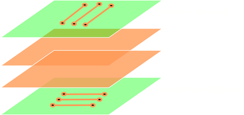 So, now you’ve got two more copper layers – what should you do with them? There are a number of ways to arrange your design, but unless you have specific reasons, it’s best to stick with the most common strategy. In this approach, the outer layers are used for signals, and the two inner layers are used as power and ground planes. Most commonly, the ground plane is closest to the component side of the PCB. Signals are then placed on the two outer layers. One convenient way to do this is to route signals in orthogonal directions on the two layers – the top layer might have primarily vertical traces, while those on the bottom would be mostly horizontal. To get to somewhere on a diagonal, you take a Manhattan-distance path, alternating between layers. This increases the achievable signal density, and is a good starting point for iterating on a design.
Connections between the layers are made with vias, just like in two-layer stackups. To power an IC, for instance, the pin may be broken out with a short, wide trace to a via which connects to the power plane. Better yet, you can create a small “power island” made from a copper pour on the component side which is connected to the plane through several vias, adding one or more bypass capacitors nearby for rock-solid power supply. With multi-layer PCBs, there are different varieties of via, although in hobbyist-level offerings, you typically will be limited to the more familiar type that goes through all layers of the board. In more advanced board processes, you can also have blind vias which only connect outer layers to an inner layer, or buried vias which only connect inner layers.
OK, you’ve chosen to go with a four-layer stackup and the standard layer arrangement. What does this buy you? First, power distribution is greatly simplified and improved. Nearly solid planes, broken only by vias, have very low inductance and resistance, improving power quality, plus there’s no need to fit wide power traces onto the signal layers. Anywhere you need VCC or GND, just drill down for it. Without power traces on the outer layers, there’s that much more room for signal traces.
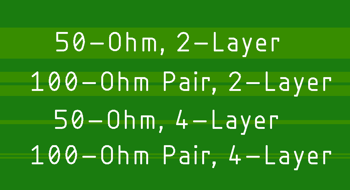
There are even more benefits for RF or high-speed digital designs. A 50-ohm trace on a typical two-layer board is around 110 mils wide. On the example four-layer stackup shown above, that drops to 14 mils, nearly a factor of eight improvement in density just from the track width. Differential digital signal pairs can also be improved, shrinking their footprint by a factor of four in this example. These advantages can easily result in more compact, yet easier-to-route designs, saving you board area and precious design time.
Some of the biggest pluses of moving to four-layers may not be immediately obvious, but there are more advantages to the small distance between the inner copper layers and their respective outer ones. Keeping the signal traces close to a power or ground plane increases the coupling between them, and decreases the signal loop area including the current return path. These factors decrease radiated emissions and improve signal integrity. If it’s just a hobby project, you may not be thinking of emissions testing, but if you ever want to get your design certified for sale, it can be a showstopper issue. Improved signal integrity, on the other hand, means you have a greater chance of a successful high-speed design the first time.
These advantages can be dramatic and almost come automatically. As a great example, Dave Jones over at eevblog recently posted a video where he took an existing two-layer design, the Gigatron TTL microcomputer, and changed it to four-layers simply by adding power and ground planes in between the existing signal layers. When he noise-tested the PCB, emissions from the four-layer version were greatly reduced compared to the original design.
So, that all sounds awesome, but surely there must be some disadvantages to four-layer designs. Yes, but they’re relatively minor. First, four-layer boards cost more than two-layer boards on a per-area basis. Typical numbers are from 1.5 x to 2 x the cost for boards of equal quality, not counting the really cheap “deals” on leaded HASL finish two-layer prototype-grade services. This metric can be a little misleading, however. A four-layer design may be smaller than the corresponding two-layer version, negating some of the per-area cost difference. The cost of the PCB may also be a small fraction of the total BOM, so doubling it will only add a small incremental cost.
For one-off and personal projects, using a four-layer stackup may pay for itself in the time and effort saved routing the design. If you’re planning a production run, four layers may still make sense, even if it’s just for a prototype that you can later try to cost-reduce into two-layers. Get it working quickly, then optimize later.
Another perceived disadvantage is the increased production time for the more complex four-layer process. This may have been more of an issue in the past, as the times are becoming more comparable lately. OSH Park, for instance, ships 90% of its two-layer orders in 8 calendar days, and an equivalent proportion of their four-layer ones in 9 days, with the times expected to equalize within the next few months. Combined with real-life shipping times, minor differences like this are completely inconsequential.
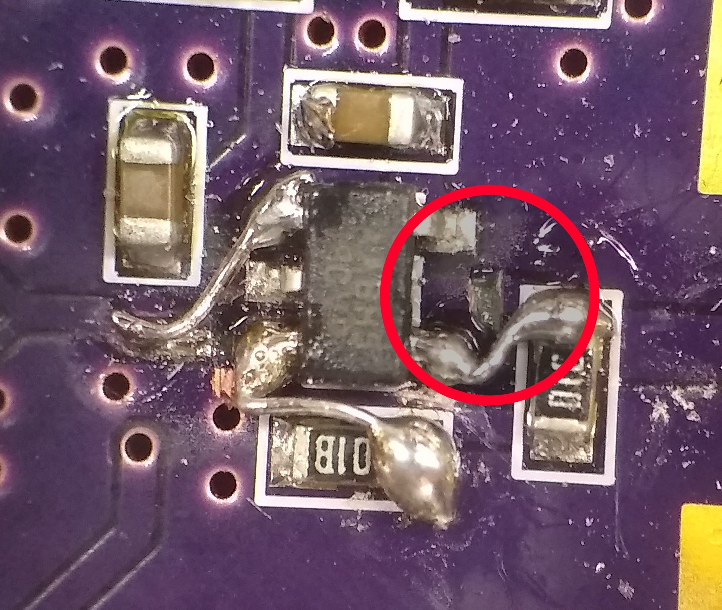
Besides time and cost, there may also be minor functional drawbacks to four-layer designs. Reworking a four-layer board to correct mistakes in a prototype can be more difficult than fixing a two-layer version. Since the inner layers are so close to the outer ones, it doesn’t take much extra force to accidentally cut into a ground or power plane when surgically disconnecting a signal trace. This can cause either side of the trace to short to the plane. A light touch and a thorough check with a microscope is advised. On the other hand, if you’ve routed signal traces on inner layers for some reason, re-working the board may be next to impossible: another reason to stick power planes in there.
Routing a four-layer PCB can involve some new twists, requiring a little extra thought. For instance, in the four-layer stackup described above, signals on the bottom layer are referenced to the power plane; their return current must flow through the plane to the nearest bypass capacitor to find its way back to ground. If you’re switching layers often with high-speed signals, you may need to add additional bypass capacitors between the planes at strategic points on the board to shorten these return paths and keep signal loop areas small. The upside is that doing so is simply a matter of placing the caps and dropping a few vias to connect them to the internal planes.
Finally, your favorite PCB layout tool may not support four-layer boards. Eagle’s free version is limited to two layers, as is Fritzing. If you use a hobbyist-oriented package, you’ll need to verify that it will do more layers. This may be the most compelling reason I’ve heard yet to get started with KiCAD.
Given all the advantages that four-layer designs bring and the minimal extra cost, it’s probably worthwhile to evaluate if any of your current or future designs would benefit from stepping up. Personally, I usually start with four-layer designs these days. About the only time I use two-layers is for extremely simple boards, or when I need them quickly, since I can get rush two-layer orders in about a week (coincidentally at the same price as normal turn-time four-layers).
There’s no reason to stop at four-layers, either. Similar arguments can be made for moving to higher-layer stackups. For a particularly interesting take, check out Kerry Scharfglass’s talk at last year’s Hackaday Superconference, where he describes spending an extra $130 to move his 500-piece order from four-layer to six-layer and saving an estimated 20-30 hours of design time.
You might be see a similar savings on your next project. Give it a try.
[Thanks to Laen and Drew at OSH Park for their insights and data.]
Stuck Designing Two-Layer PCBs? Give Four Layers a Try!
Source: HackADay